Silicon has four valence electrons, so the valence electrons from a pair of silicon atoms together form a completed shell level of eight electrons.
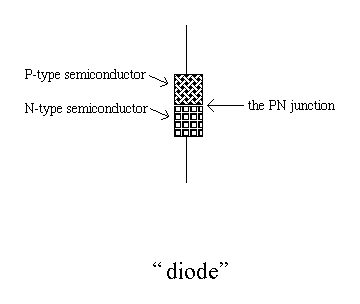
But when you mix silicon with traces of boron or indium, which are elements with only three valence electrons, you get what's called a "P-type semiconductor", which has an increased ability to conduct a positive electric current. Since the trace elements have only three valence electrons, the outer levels will have seven electrons, not eight, so they have a "hole".
Alternatively, if you mix silicon with traces of phosphorous or arsenic, which are elements with five valence electrons, you get what's called an "N-type semiconductor", which has an increased ability to conduct a negative electric current, because it has a surplus of electrons.
These substances are still both electrically neutral. The fewer electrons in the orbitals is matched by fewer protons in the nuclei, etc.
The useful bit happens when we put them together:
The "diode effect" is the name of the effect which happens at the PN junction in which we get either a very high or a very low resistance, depending upon which side has a greater voltage. If the 'P' side has a higher voltage, we have a very low resistance. If the 'N' side has a higher voltage, we have a very high resistance.
We can put two diodes together to make an "NPN transistor":
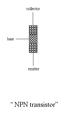
An NPN transistor is like an electrically-controlled switch. If there is current at the base, then current can flow from the collector to the emitter. If there is no current at the base, then current cannot flow from the collector to the emitter.
So, does the following make an 'AND' gate?
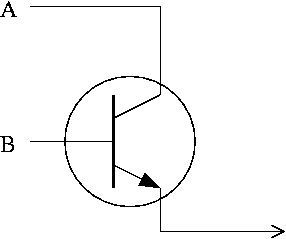
Not quite. If you measure the voltage at the output when 'A' and 'B' are both logic 1, you'll see it's lower than the input voltages. So if you make a big circuit out of these, by the time you're near the outputs of the circuit you won't have enough of a difference between logic 0 and logic 1.
And that's not the only problem. NPN transistors rely on a large difference in voltage. If we have some spare voltage around in our circuit, which we always will if we connect things up this sloppily, we're going to get some current flowing from emitter to base. Etc.
So this expanded version is not a lot better:
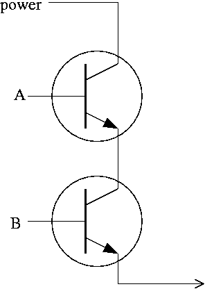
That solves the output-quality problem: If the AND gate is supposed to be outputting a logic 1, it will give a good quality connection from the power to the output.
But if the AND gate is supposed to be outputting a logic 0, it will not be grounding the output. No good.
Here is the standard TTL NAND gate... sorta. I've left the actual resistance values unspecified (and they're important, especially that some combinations are greater than others), and I've also omitted a crucial diode.
But this gives the basic idea. You can find a non-simplified TTL NAND gate in many places on the web, such as in the wikipedia article.
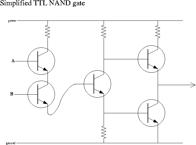
The transistor in the top right is the "output a 1" transistor and the transistor in the lower right is the "output a 0" transistor. Exactly one of these two transistors will be active (powered at the base), as decided by the middle transistor.
Wait, we've switched from AND to NAND!
Actually, that's good. NAND is a "basis" -- every boolean function can be made only out of NANDs -- whereas AND is not.